

Physical Vapor Deposition: Classification, Principles, and Applications
Release time:
15 May,2024
Summary
Physical Vapor Deposition (PVD) is a novel thin film deposition technology that physically transforms the target material (target) into gas or plasma under vacuum, and then deposits it on the substrate surface. It is currently one of the main surface manufacturing technologies.
PVD was developed as early as the beginning of the 20th century and has broad application prospects with its development. Its process is more environmentally friendly, the cost is easy to control, the consumption of consumables is low, the prepared film is relatively uniform and dense, and the film-substrate bonding force is strong. It is widely used in various additive manufacturing fields. Samples with various properties can be prepared according to the needs of the processor, such as: wear resistance, corrosion resistance, conductivity, insulation, piezoelectricity, magnetism, hydrophilicity, hydrophobicity, etc.
The basic principle of physical vapor deposition technology can be divided into three process steps:
(1) Vaporization of the coating material: Even if the coating material evaporates, sublimates, or is sputtered, it is also through the vaporization source of the coating material;
(2) Migration of electroplated material atoms, molecules, or ions: After the collision of atoms, molecules, or ions supplied by the vaporization source, various reactions occur;
(3) Coating atoms, molecules, or ions are deposited on the substrate 。
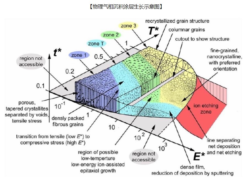
PVD is a surface treatment technology that physically prepares the target material on the surface of the target substrate. All this is done in a vacuum. PVD technology mainly includes three major categories: vacuum evaporation coating, vacuum sputtering coating, and vacuum arc ion plating.
In recent years, the development of thin film technology and thin film materials has been rapid and eye-catching. On the basis of the existing technology, ion beam enhanced deposition technology, electric spark deposition technology, electron beam physical vapor deposition technology, and multilayer jet deposition technology have emerged one after another.
1. Vacuum evaporation
The principle of vacuum evaporation coating is relatively simple, including electron beam evaporation coating, resistance evaporation coating, arc evaporation coating, laser evaporation coating, and other methods.
The main method is to heat the target material into gas evaporation or vaporization in a vacuum. Usually, the heating source is located below the target material, and the target substrate is located above the target material. The target molecules will rise under the action of thermal energy, thus depositing on the target substrate. More and more target gas molecules gather on the target substrate, and they will grow into a dense thin film.
The difference between different evaporation coating methods lies only in the different heating methods.
Resistance evaporation coating uses Joule's law to provide thermal energy to the resistor. When the temperature of the resistor becomes higher, it will heat the target material and transform it into gas molecules.
The electron beam evaporation coating method is slightly different. It uses an electron beam evaporation source to emit an electron beam and project it onto the target surface. The target material is generally placed in a crucible, and the heating area is also smaller. The electron beam can be heated to above 1000K, which can melt all common materials.
2. Vacuum sputtering coating
Sputtering coating refers to the process in which the surface atoms of the target material obtain enough energy to escape under vacuum conditions by bombarding the target material surface with functional particles, which is called sputtering. The process of depositing the sputtered target material onto the substrate surface is called sputtering coating.
The principle of magnetron sputtering is shown in the figure, where M represents metal particles. Free electrons are accelerated by the electric field and fly towards the anode. In this process, they collide with Ar atoms, causing them to lose their outer electrons and release Ar+ and free electrons. Ar+ flies towards the cathode under the action of the electric field, hits the target, knocks off the target atoms, and secondary electrons. Free electrons may also collide with Ar+ during flight, causing them to return to neutrality. However, in this process, electrons return from the excited state to the ground state and release energy. This part of the energy will be released in the form of photons, and because a large number of photons are released, the plasma will appear "luminous".
Different incident ions (Ar+) have different energies and achieve different effects. When the incident ion energy is low, the incident ion deposition (ion beam deposition) method is mainly used; when the energy is moderate, the target atoms are sputtered; when the incident ion energy is too high, they will be injected or diffused into the target.
3. Arc ion plating
The basic principle of arc ion plating (AIP) is arc discharge. The furnace is pumped to a lower vacuum, and then a certain intensity is applied to the arc needle. The current is attracted to the target surface, and finally, the strong current causes the target surface to evaporate or vaporize. The target atoms gain kinetic energy and diffuse to the substrate surface, where they are adsorbed, nucleated, and finally grow into a thin film.
The main characteristics of arc ion plating are: high working vacuum degree, low gas impurity pollution; fast deposition rate, thicker film; high ionization rate of deposited particles, high ion energy; simple deposition device, small substrate temperature rise.
Based on the principle and characteristics of arc ion plating, it also has certain disadvantages: due to the high current intensity and large energy provided by arc ion plating, metal droplets are easily generated on the surface of the metal target material, and metal droplets directly deposited on the substrate surface will reduce the performance of the coating and the bonding force between the film and the substrate; because the arc needle must be subjected to a strong current, the target material must be made of conductive material, and the selectivity is poor.
4. Ion beam enhanced deposition technology
Ion beam enhanced deposition technology is a new type of material surface modification technology that integrates ion implantation and thin film deposition. It refers to the formation of a single substance or compound film layer by bombarding and mixing with an ion beam of a certain energy during gas phase deposition coating.
In addition to retaining the advantages of ion implantation, it can also continuously grow film layers of arbitrary thickness under low bombardment energy, and can synthesize compound thin films with ideal chemical ratios at room temperature or near room temperature (including room temperature and normal temperature). New film layers that cannot be obtained by pressing).
The process temperature of this technology is low (<200°C), and the bonding force to all substrates is strong. High-temperature phases, metastable phases, and amorphous alloys can be obtained at room temperature. The chemical composition is controllable, and the growth process is easy to control. The main disadvantage is that the ion beam is direct and it is difficult to process surfaces with complex shapes.
5. Electric Discharge Deposition Technology
Electric discharge deposition technology involves the instantaneous, high-frequency release of high-energy electrical energy stored in a power source between a metal electrode (anode) and a metal substrate (cathode) through the air between the electrode material and the substrate. Ionization creates a channel, generating a momentary high-temperature, high-pressure micro-region on the substrate surface. Simultaneously, the ionic electrode material melts and penetrates into the substrate matrix under the action of a micro-electric field, forming a metallurgical bond.
EDM deposition is a process between welding and sputtering or elemental permeation. Metal deposited layers processed using electric discharge deposition technology have high hardness and good high-temperature resistance, corrosion resistance, and wear resistance. The equipment is simple and widely applicable. The bond between the deposited layer and the substrate is very strong and generally will not peel off. The workpiece will not be annealed or deformed after processing. The thickness of the deposited layer is easy to control, and the operating method is easy to master. The main disadvantages are the lack of theoretical support and the fact that the operation has not yet been mechanized or automated.
6. Electron Beam Physical Vapor Deposition Technology
Electron beam physical vapor deposition technology uses a high-energy density electron beam to directly heat and evaporate materials, allowing the evaporated material to deposit on the substrate surface at a lower temperature.
This technology has advantages such as high deposition rate (evaporation rate 10kg/h~15kg/h), dense coating, easy precise control of chemical composition, columnar crystal structure, no pollution, and high thermal efficiency. The disadvantages of this technology are expensive equipment and high processing costs. Currently, this technology has become a research hotspot in various countries.
7. Multilayer Spray Deposition Technology
Compared with traditional spray deposition technology, an important feature of multilayer spray deposition is that the motion of the receiver system and the crucible system can be adjusted, making the deposition process uniform and the trajectory non-repetitive, thus obtaining a flat deposition surface.
Its main characteristics are: the cooling rate during the deposition process is higher than that of traditional spray deposition, and the cooling effect is better; large-size workpieces can be prepared without affecting the cooling speed; the process operation is simple, and it is easy to prepare workpieces with high dimensional accuracy, uniform and flat surface; high droplet deposition rate; the microstructure of the material is uniform and fine, with no obvious interface reaction, and good material properties.
Currently, thin film technology, as a new material preparation technology, has transitioned from exploratory research in the laboratory to large-scale industrial production and is penetrating various industries. Its application range and role are constantly expanding and deepening.
This new technology not only involves basic disciplines such as physics, chemistry, crystallography, surface science, and solid-state physics, but is also closely related to technical fields such as vacuum, metallurgy, and chemical engineering.
As an important component of materials science, thin film technology has received widespread attention and research. In order to continuously improve the development level of thin films, it is necessary to attach importance to the basic theoretical research of thin film technology and strive to elevate general skills and experience into scientific theories.
In physical vapor deposition, precise control of gas flow is crucial to the quality and performance of the thin film. 。
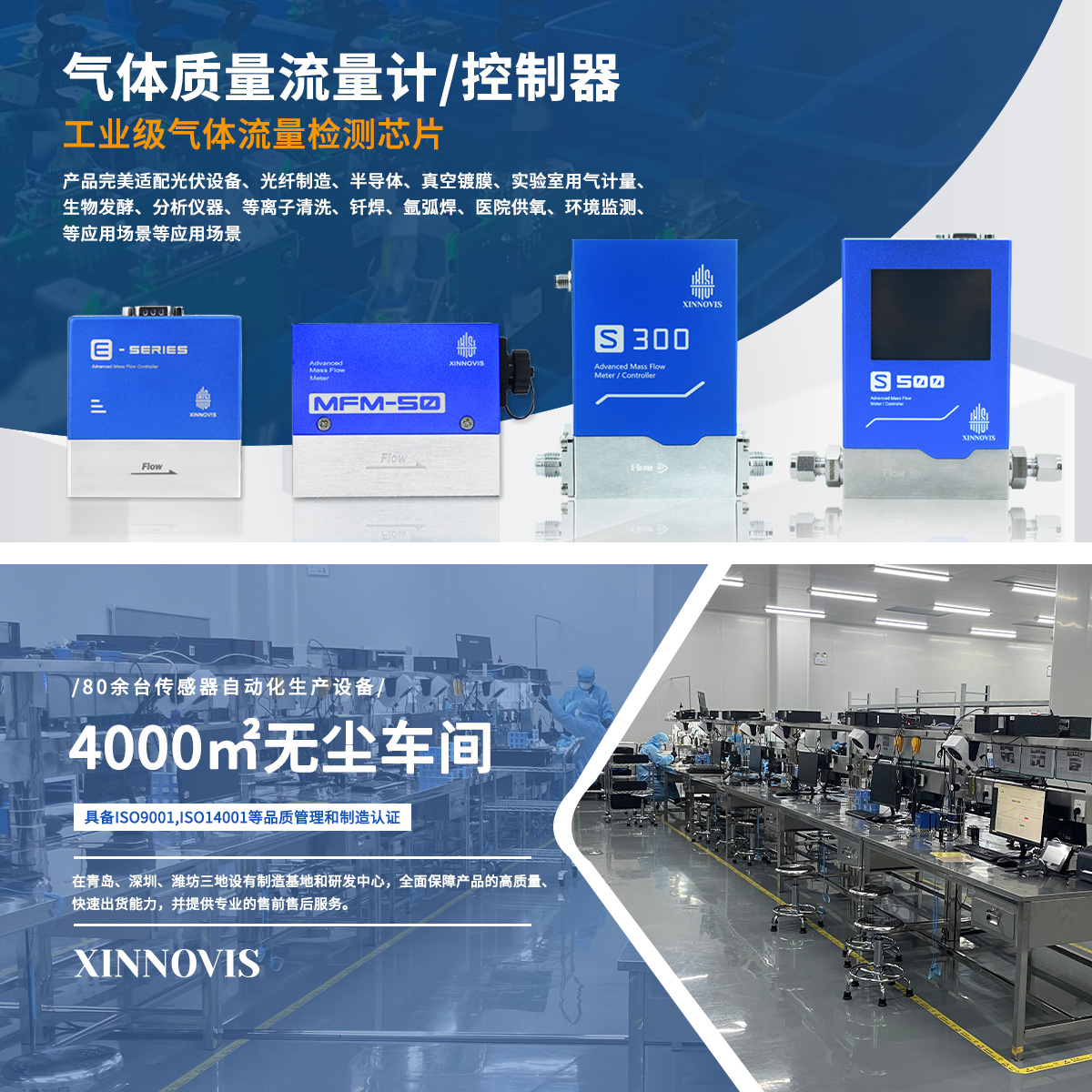
Qingdao Xinnovis's self-developed MFC (mass flow controller) has outstanding advantages such as low temperature drift, pollution resistance, and high cost-effectiveness. The use of advanced MEMS technology improves measurement accuracy, consistency, and reliability. Compared with traditional capillary flow meters, the MEMS-based MFC has a higher signal-to-noise ratio, smaller thermal capacity and thermal response, and higher processing accuracy and reliability. Whether in the semiconductor industry or other fields, Qingdao Xinnovis's self-developed MFC can stably and accurately control gas flow. The company's products have undergone rigorous testing and have excellent anti-electromagnetic interference capabilities, allowing them to operate normally in complex electromagnetic environments.
More News

Tel: 400 006 6550
Office Address: 12. Stock, Gebäude I, Internationaler Innovationspark, Nr. 177 Songling Road, Laoshan District, Qingdao