

This article is all you need to know about PECVD!
Release time:
28 Jun,2024
Summary
PECVD What is it
Plasma-enhanced chemical vapor deposition (PECVD) is a common thin-film deposition technique in the semiconductor industry. This technology combines the basic principles of chemical vapor deposition (CVD) with plasma technology to produce high-quality films and precisely control their properties. Unlike traditional CVD technology, PECVD uses plasma to improve deposition efficiency, allowing material deposition at lower temperatures.
In PECVD technology, a low-temperature plasma under low pressure triggers a glow discharge at the cathode in the deposition chamber. This process may involve heating the sample to a set temperature using other heating devices and introducing a specific amount of process gas. These gases undergo various chemical reactions under the action of plasma, ultimately forming a solid-state film on the sample surface. Plasma-enhanced chemical vapor deposition (PECVD) technology can enhance the reactivity of organic and inorganic chemical monomers, allowing the use of a variety of precursor materials, including those traditionally considered inert, to deposit various films. PECVD technology can use solid, liquid, or gaseous precursors, making it a convenient, rapid, and solvent-free method for producing film coatings.
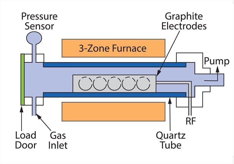
In the PECVD process, plasma generation is typically achieved by applying a voltage across electrodes in a low-pressure gas environment. PECVD systems can generate plasma in a variety of ways, such as radio frequency (RF), medium frequency (MF), pulsed direct current, or direct direct current. These power supplies provide energy to the gas or vapor, generating electrons, ions, and neutral radicals.
Low-temperature processing: PECVD technology can deposit films at lower temperatures than traditional CVD technology, which is particularly important for semiconductor manufacturing, as high temperatures can damage delicate device structures. Excellent film uniformity: PECVD technology can form films with highly consistent thickness and composition on the substrate, this uniformity is crucial for device performance and reliability. High deposition rate: PECVD has a significantly higher deposition rate than traditional CVD technology, making the production of semiconductor devices more efficient and economical. Wide range of materials: PECVD can deposit a variety of materials, including insulators, conductors, and semiconductors, its versatility makes it suitable for a variety of applications in semiconductor manufacturing. In-situ process monitoring: PECVD systems are typically equipped with real-time monitoring capabilities, allowing for immediate adjustment of deposition parameters to improve film properties.
PECVD Advantages
Low-temperature deposition: Compared to traditional CVD technology, PECVD can deposit films at lower temperatures, which is crucial for semiconductor production, as high temperatures can damage precision equipment. Excellent film uniformity: PECVD technology can form uniform films with consistent thickness and composition on the substrate, which is extremely important for improving device performance and reliability. Fast deposition speed: The deposition rate of PECVD is higher than that of traditional CVD technology, making the manufacturing of semiconductor devices more efficient and economical.
Wide range of applicable materials: PECVD can deposit a variety of materials, including insulators, conductors, and semiconductors. Its versatility is suitable for various applications in semiconductor manufacturing. In-situ process monitoring: PECVD systems are usually equipped with real-time monitoring functions, which can adjust deposition parameters in real time to improve film properties.
PECVD Future Outlook
PECVD technology is expected to continue to play a key role in the electronics field. Its market growth is driven by several emerging applications and technological advances, especially the development of new materials: PECVD technology can deposit a variety of materials, such as metals, semiconductors, dielectrics, and polymers. This versatility makes PECVD the preferred technology for various applications, including advanced packaging, optoelectronics, and microelectronics.
PECVD technology can be used in conjunction with other deposition technologies such as physical vapor deposition (PVD) and atomic layer deposition (ALD). Such combinations can form complex multilayer structures to produce devices with specific functions and higher efficiency. In addition, current research and development activities are mainly focused on improving the performance of PECVD systems and the breadth of their applications. Researchers hope to develop new processes and materials to manufacture next-generation devices. It is expected that in the next few years, with the increasing demand for advanced electronic products, the development of new materials and technologies, and the integration of PECVD technology with other deposition methods, its market will expand significantly.
Qingdao Xinnovis independently developed MFC (gas mass flow controller) In PECVD or other applications, It has demonstrated several advantages, including electromagnetic interference resistance, strong anti-pollution ability, and high cost-effectiveness. This product utilizes advanced MEMS technology to significantly improve measurement accuracy, consistency, and reliability. Compared with traditional capillary flow meters, MFC with MEMS chips exhibits higher signal-to-noise ratio and faster response time, while providing higher processing accuracy and reliability. Qingdao Xinnovis's MFC can stably and accurately control gas flow. The product has undergone rigorous testing and has excellent electromagnetic interference protection capabilities, and can still operate normally in complex electromagnetic environments.
More News

Tel: 400 006 6550
Office Address: 12. Stock, Gebäude I, Internationaler Innovationspark, Nr. 177 Songling Road, Laoshan District, Qingdao