

Advantages and market applications of MEMS sensors: mass flow meters
Release time:
24 Feb,2022
Summary
MEMS stands for Microelectromechanical Systems. Mi croElect rom echanicalSystem. It refers to devices with dimensions of a few millimeters or even smaller. Sensors devices. Their internal structures are generally at the micrometer or even nanometer level, forming an independent intelligent system. In simple terms, MEMS miniaturizes the mechanical components of traditional sensors, then uses three-dimensional stacking technologies, such as three-dimensional silicon through-silicon vias (TSV), to fix the devices on a silicon wafer (w afe r), and finally adopts specially customized packaging forms according to different application scenarios, ultimately forming silicon-based sensors through cutting and assembly. Benefiting from the cost advantages brought by the mass production of IC silicon wafers, which is unattainable for ordinary sensors, MEMS also possesses miniaturization and high integration that ordinary sensors lack.

MEMS mainly involves microfabrication technology, mechanics/solid-state acoustics theory, thermal flow theory, electronics s, biology, etc. The characteristic length of MEMS devices ranges from 1 millimeter to 1 micrometer. In comparison, the diameter of a human hair is approximately 50 micrometers.
The main advantages of MEMS sensors are their small size, light weight, low power consumption, high reliability, high sensitivity, and ease of integration. They are the main force behind miniature sensors and are gradually replacing traditional mechanical sensors. Research is being conducted in almost all fields, including consumer electronics, automotive industry, aerospace, machinery, chemical industry, and medicine.
2. MEMS is the only choice to replace traditional sensors.
The conversion from analog to digital, from large size to miniaturization, and the resulting high integration are the eternal pursuit of all modern industrial development. MEMS is considered the only possible choice to replace sensors, and may also be one of the most important choices for building the future Internet of Things sensing layer sensors. It has the following advantages:
Advantage 1: Miniaturization
MEMS devices are small in size, with individual MEMS sensors typically measured in millimeters or even micrometers, and are lightweight and low-power. Miniaturization also results in mechanical components with low inertia, high resonant frequency, and short response times. The higher surface-to-volume ratio of MEMS can improve the sensitivity of surface sensors.
Advantage 2: Mass Production
Taking a single 5mm*5mm MEMS sensor as an example, approximately 1000 MEMS chips can be simultaneously cut from a single 8-inch silicon wafer using silicon microfabrication technology. Mass production significantly reduces the production cost of individual MEMS.
Advantage 3: Integration
Generally, a single MEMS often integrates a mechanical sensor packaging along with ASIC chips to control the MEMS chip and convert analog signals to digital output. The integration of microsensors, microactuators, and microelectronic devices can produce highly reliable and stable MEMS. With the development of MEMS technology, there is a current trend towards integrating more functions into a single MEMS chip to achieve higher integration.
Advantage 4: Multidisciplinary Crossovers
MEMS involves electronics, mechanics, materials, manufacturing, information and automatic control, physics, chemistry, and biology, and integrates many cutting-edge achievements in today's scientific and technological development. MEMS is one of the most important choices for building the basic physical sensing layer sensors of the Internet of Things.
Because the Internet of Things, especially wireless sensor networks, is highly sensitive to the physical size, power consumption, and cost of devices, the miniaturization of sensors is crucial to the development of the Internet of Things industry. MEMS microelectromechanical systems combine traditional semiconductor processes, using microtechnology to manufacture micro-machines on chips and integrating them with corresponding circuits into a single unit. It is based on semiconductor manufacturing technology and mass production can meet the huge demand and low-cost requirements of the Internet of Things for sensors.
The scale of fabless companies in China's MEMS industry is relatively small, but the market size has great potential for development. Facing the huge domestic consumer electronics market, self-production and sales to meet the needs of some domestic low-to-mid-end markets is also a shortcut for domestic fabless companies. Chinese MEMS design companies are mainly concentrated in East China, accounting for about 55% of the total number of enterprises nationwide, with Shanghai, Suzhou, and Wuxi as the main industrial centers.
From a market perspective, China has the world's largest integrated circuit market. Coupled with the catalysis of the Internet of Things, the domestic market's demand for accelerometers, high-precision pressure sensors ,silicon microphones, gyroscopes 、 radio frequency instruments, gas sensors and electronic compasses is becoming increasingly urgent.
The MEMS industry chain is complex and involves numerous manufacturers. Design, manufacturing, and packaging and testing manufacturers are actively deploying MEMS, and China has gradually formed a complete MEMS industry chain.
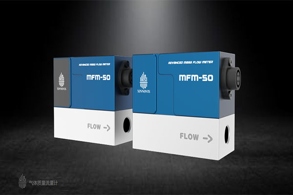
The Qingdao Xinnovis MFM-50 series gas mass flow meter is specifically designed for high-precision measurement of gas flow. This series of flow meters uses industry-leading flow sensing chips, combined with an aviation aluminum polished gas flow path design, and incorporates the company's core calibration and compensation algorithms to achieve high-precision measurement of various clean, dry, and non-corrosive gases. The typical accuracy of this product is 1% within 20 SLM and 1.5% at 50 SLM. The range ratio is better than 100:1. The range of this series of products is selectable from 100 SCCM to 800 SLM (other ranges can be customized upon inquiry), and it is equipped with an LCD display, digital and analog outputs, facilitating on-site and remote debugging. This product is low-cost, easy to install, and does not require additional temperature and pressure compensation.
More News

Tel: 400 006 6550
Office Address: 12. Stock, Gebäude I, Internationaler Innovationspark, Nr. 177 Songling Road, Laoshan District, Qingdao