

ALD, critically important!
Release time:
24 May,2024
Summary
Atomic layer deposition (ALD) is a crucial tool used in semiconductor manufacturing, particularly at current nodes for transistor and interconnect fabrication. While ALD was previously considered too slow to be practical, its value has been affirmed as the need for precise control of composition and thickness has increased, making the extra time spent on ALD deposition in the manufacturing process worthwhile.
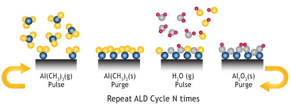
ALD is a variant of chemical vapor deposition, initially widely introduced into the semiconductor industry for the fabrication of high-k hafnium oxide gate dielectrics. Similar to chemical vapor deposition (CVD), ALD is also a conformal process, with deposition occurring on all surfaces exposed to the precursor gases. However, in ALD, the reaction is self-limiting.
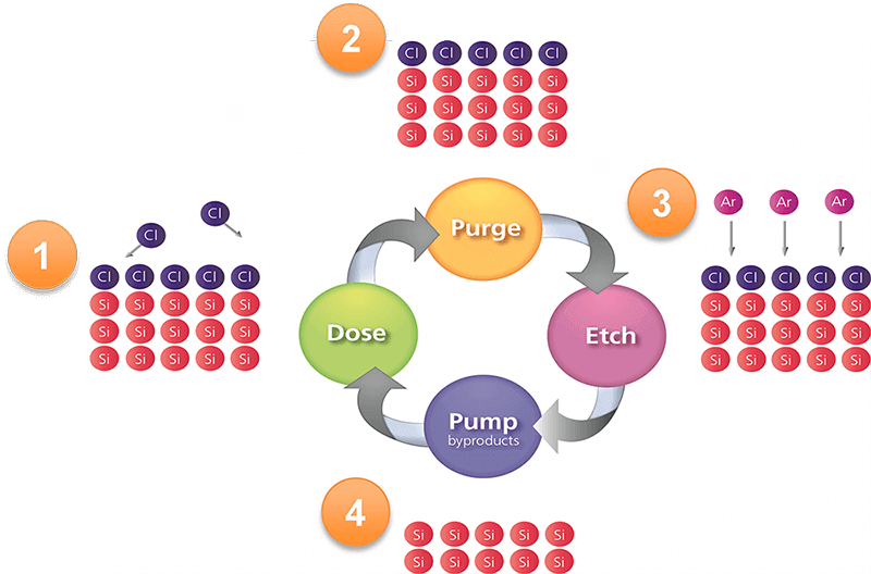
ALD works as follows: First, precursor gas A is introduced into the processing chamber and adsorbs onto all available substrate surfaces. Once all surface sites are occupied, further adsorption does not occur. Any remaining precursor gas is then purged using an inert purge gas (typically nitrogen or argon), and a second precursor B is introduced. Precursor B reacts with the already chemisorbed precursor A to form the desired thin film. Once all adsorbed molecules are consumed, the reaction stops. This cycle is repeated after a second purge step.
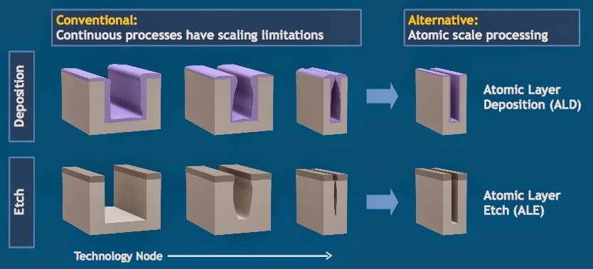
The advantages and disadvantages of ALD lie in its layer-by-layer nature. Depositing only one layer at a time allows manufacturers to control the thickness of the film very precisely. The composition of the film can be tuned by using different precursor gases in different proportions. However, the repetitive precursor/purge gas cycles are time-consuming. To improve throughput, some process adjustments can be made, such as using large furnaces to process multiple wafers at once or using plasma activation to accelerate film formation. However, the maximum practical thickness of ALD films is usually limited, while opportunities for ALD are constantly increasing as transistors shrink and the demand for complex structures increases.
One of the successful applications of ALD in semiconductor manufacturing is hafnium oxide (HfO2). The precursors for HfO2, HfCl4 and water, are chemically simple small molecules whose byproducts are easily volatile and removable. However, the ALD processes for many other materials can be more complex, for example, silicon dioxide often uses aminosilane precursors, while metal nitrides typically require complex metal-organic precursor gases. In selective deposition processes, adding ligands to the precursor molecules can alter their vapor pressure or reactivity, or promote adhesion to the substrate, thereby improving selectivity between the growth surface and the non-growth surface. However, larger molecules may have difficulty penetrating smaller features, and removal of byproducts may also be difficult.
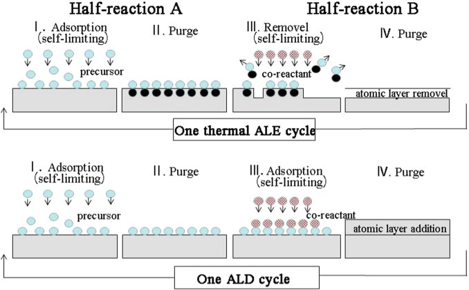
In addition, atomic layer etching (ALE) can be used to remove unwanted materials. The operating steps of ALE are similar to ALD, achieved through a series of cycles. The first half of the cycle reacts with the existing surface, weakening the interaction with the underlying layer, and then the byproducts are removed by an inert purge gas. The second half of the cycle is a selective adsorption step, where precursor molecules react with the weakened surface and form volatile products, thereby removing the unwanted material layer by layer.
Atomic layer deposition (ALD) is an important process used in semiconductor manufacturing that allows for precise control of film thickness and composition. While ALD is relatively slow, its advantages include high controllability and selectivity. As technology advances, ALD is increasingly used in semiconductor manufacturing, helping to achieve smaller, faster, and higher-performance chips.
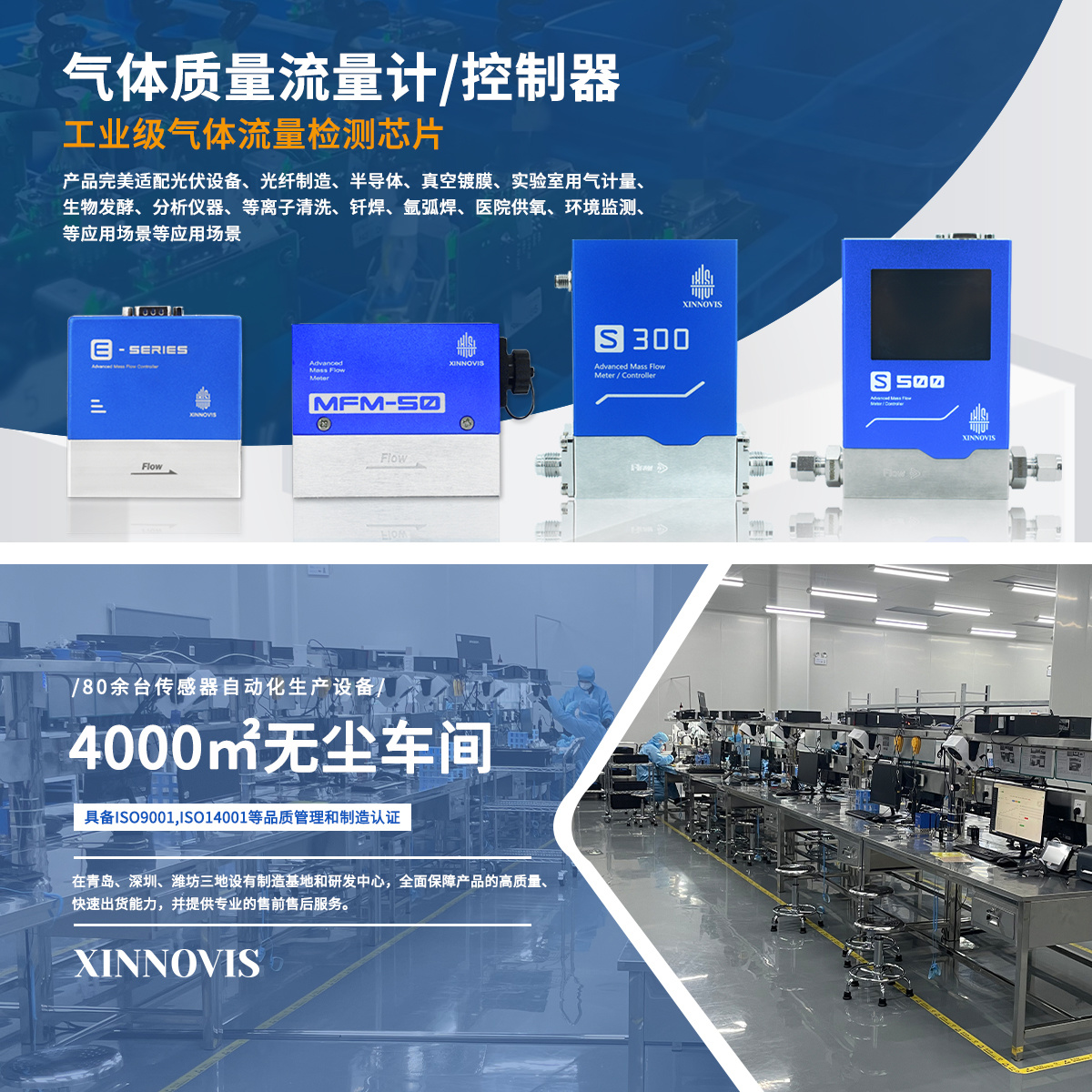
In the technological applications oriented towards atomic layer deposition (ALD) and atomic layer etching (ALE), the gas mass flow controllers (MFCs) independently researched and developed by Qingdao Xinnovis play a crucial role. This MFC, with its advantages of low temperature drift, pollution resistance, and high cost-effectiveness, has become the preferred choice in the industry. We use MEMS technology to improve the measurement accuracy, consistency, and reliability of the MFC.
Compared to traditional capillary flow meters, the MEMS-based MFC can achieve higher signal-to-noise ratio, smaller
heat capacity, faster thermal response, and higher processing accuracy and reliability. This is crucial for precise ALD and ALE process control, as both processes require precise and stable gas flow control.
In the semiconductor industry, whether it is achieving atomic-level thin film deposition in high-precision ALD processes or accurate atomic-level etching in ALE processes, Qingdao Xinnovis's MFC has demonstrated its unparalleled stability and precision. In addition, our products have passed rigorous testing and have excellent anti-electromagnetic interference capabilities, allowing them to operate normally in complex electromagnetic environments and ensuring the stable progress of ALD and ALE processes.
For atomic layer deposition and atomic layer etching processes that require high precision and stability, Qingdao Xinnovis's self-developed MFC is undoubtedly the industry's choice.
Previous:
More News

Tel: 400 006 6550
Office Address: 12F, Building I, International Innovation Park,
177 Songling Road, Laoshan District, Qingdao, Shandong, China