

Research on the chip structure design of MEMS flow sensors
Release time:
23 Jun,2022
Summary
MEMS chip development. MEMS technology, since the advent of the transistor era, has rapidly developed and grown over several decades. It integrates miniature mechanics, microsensors, microactuators, signal processing, and intelligent control based on microelectronics technology. From initial pressure sensors to advanced miniature devices such as automotive airbags, it has been widely applied in various fields. Compared with traditional mechanical equipment, MEMS has insurmountable advantages, such as generalization, miniaturization, diversification, stability, integration, and mass production. Miniature instruments manufactured using MEMS technology are very promising in environmental detection, analysis, and processing. They are mainly composed of chemical sensors, biosensors, and data processing systems, forming miniature measurement and analysis equipment. Their advantages include small size, low cost, and low power consumption. The development of MEMS technology has had a profound impact on information technology. In recent years, MEMS has gradually penetrated into the field of optical communication, forming a new research field combining micro-optics, microelectronics, micromechanics, and materials science, namely micro-optoelectromechanical systems. Various micro-pumps, micro-valves, micro-tweezers, micro-grooves, and micro-flow meters made using micro-fabrication technology are suitable for manipulating biological cells and macromolecules. Because of the small size of MEMS devices, they can enter very small organs and tissues while performing delicate and precise operations, thus greatly improving the accuracy of interventional therapy and reducing medical risks. Miniature instruments manufactured using MEMS technology are very promising in environmental detection, analysis, and processing. They are mainly composed of chemical sensors, biosensors, and data processing systems, forming miniature measurement and analysis equipment. Their advantages include small size, low cost, low power consumption, and portability.
1. Research on MEMS gas sensor chip preparation process. Using traditional working principles and some new effects, prioritizing crystalline materials (silicon, quartz, ceramics, etc.), adopting advanced processing technology and microstructure design to develop new sensors and sensor systems, such as optical waveguide gas sensors, polymer surface acoustic wave and quartz crystal gas sensors, research on microbial gas sensors and bionic gas sensors. With the application of new materials, new processes, and new technologies, the performance of gas sensors is becoming more perfect, making the miniaturization, miniaturization, and multi-functionalization of sensors have advantages such as long-term stability, ease of use, and low cost.
Research on MEMS flow sensor chip preparation process
a) Research on the preparation process of silicon-based porous silicon;
b) Research on the preparation process of low-stress thin films;
c) Research on the reliability and stability of metal electrical connections;
d) Research on the preparation of semiconductor coatings and process integration methods;
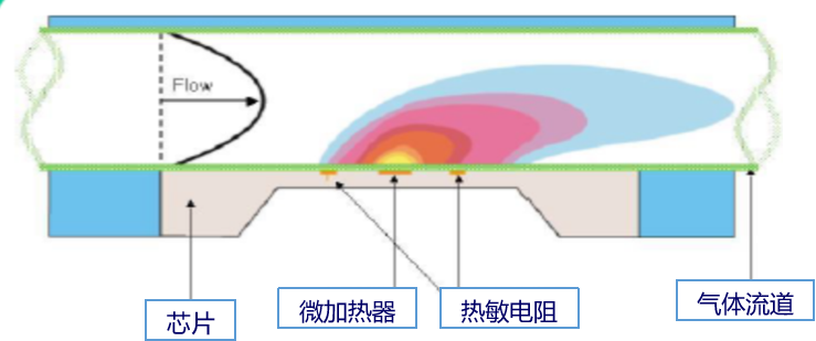
2. Development of MEMS gas flow sensor. Based on the theory proposed by scientist Thomas that "the heat absorption or release of gas is proportional to the mass flow rate of the gas." When no gas flows through the sensor chip, a stable temperature field is maintained around the sensor. When the gas medium flows through the sensor chip, the temperature field is redistributed locally due to the heat carried away by the fluid medium. The change in the local temperature field depends on the mass and flow rate of the fluid medium. The sensor integrated on the chip measures this temperature distribution. Through calibration, specially designed signal processing circuits and intelligent control software can accurately measure the actual mass flow rate of the medium.
Research on MEMS flow sensor chip structure design
a) Research on material optimization and screening;
b) Analysis of chip temperature distribution and mechanical strength;
c) Analysis of chip thermal stress;
d) Research on high-temperature interface stability of the chip;
More News

Tel: 400 006 6550
Office Address: 12F, Building I, International Innovation Park,
177 Songling Road, Laoshan District, Qingdao, Shandong, China