Recently, Zhao Yuxin's team from Xi'an Jiaotong University and Zhao Yanli from Nanyang Technological University, Singapore, published Matter an article titled "Toward Highly Trustable Miniaturized Semiconductor Gas Sensors" in the journal. This article reviews the current research pain points regarding the trustworthiness of miniaturized devices, looks forward to emerging opportunities, and provides a new perspective for future high-quality on-chip integration research of semiconductor gas sensors.
Metal oxide semiconductors (MOS) represent the best trade-off between cost and size for gas sensors. Over the past few decades, the development and rapid commercialization of low-cost microelectromechanical systems (MEMS) have led to the emergence of miniaturized MOS gas sensors based on suspended hotplate structures, as well as the application of other novel nanosensitive materials on them. Compared with traditional ceramic tube MOS gas sensors, MEMS sensors have advantages such as small size, low energy consumption, high integration, and suitability for mass production. However, at the same time, when the core electrode area of the gas-sensitive element is reduced from the millimeter-level macroscopic scale to the micrometer-level mesoscopic scale, the localized, controllable, and stable assembly of the sensitive material on the microstructure substrate becomes increasingly difficult. Poor quality control will lead to the inability of the device to exert the stable and consistent process advantages of MEMS, greatly reducing its signal effectiveness and reliability in real-world complex scenarios. At the same time, the intrinsic characteristics of nanomaterials, such as surface effects and size effects, and the synergistic properties caused by cross-scale coupling of materials/devices will also be difficult to emerge smoothly.
Since its invention in 1962, the ceramic tube MOS gas sensor has occupied a major market share in the latter half of the 20th century due to its robust technology and low cost. However, its relatively high power consumption (0.5-1W) also limits its long-term operation capability under self-powered conditions, gradually failing to meet the latest needs of low-power Internet of Things applications. With the increasing maturity of silicon-based microfabrication technology, thermally optimized MEMS suspended structure designs have been successfully implemented, enabling MOS gas sensors to enter the milliwatt power consumption era and quickly become a new favorite in academia and industry. However, in the past ten years or so, MEMS semiconductor sensors have not caused the ideal huge waves in the market and played a revolutionary replacement role.
From the technological development process of related fields, two significant characteristics can be found: First, the research focus is mainly concentrated on the sensitive materials and device design levels, while relatively less attention is paid to the scientific and technological issues in the integration process of the two, and there is no systematic methodology yet; second, gas sensor research and development work is mostly carried out based on the three principles of target molecule recognition function, gas-electric conversion function, and sensitive body utilization rate, which leads researchers to be more inclined to use the apparent signal-to-noise ratio to judge the performance. Of course, these efforts have made significant progress and achievements in improving the selectivity and sensitivity of gas-sensitive materials/devices, but it is undeniable that the requirements of most real-world application scenarios are not limited to selectivity and sensitivity.
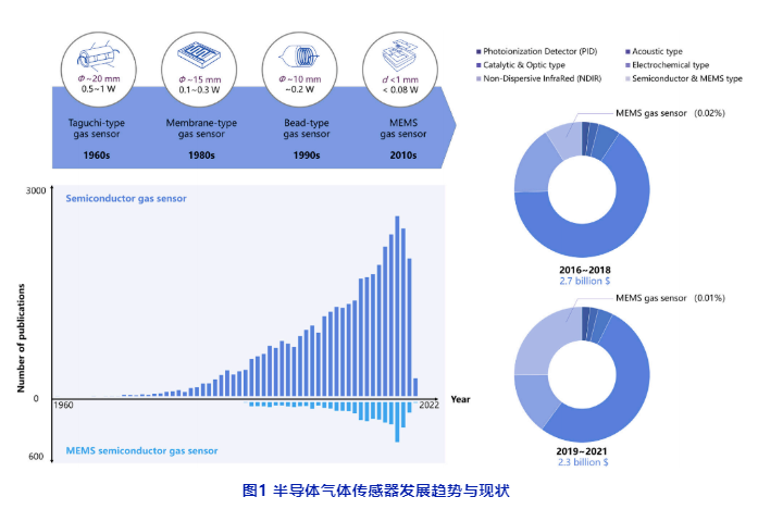
Figure 1 Development trend and current status of semiconductor gas sensors
A large number of production practices have shown that the bottleneck that restricts the widespread application of sensors and prevents them from producing disruptive social impacts as expected often lies in the reliability and consistency of the "gas-electric" conversion signal: the data chaos derived from false alarms and false positive signals will continue to accumulate and amplify with the large-scale use of sensing equipment, causing the dilution of real information and bringing disruptive interference to the fine-grained spatiotemporal judgment of the target environment. Therefore, the differences in quality control between different devices, and the stability changes of the same device in different time domains, are important challenges hindering the practical application of MEMS gas sensors. In particular, as the characteristic size of the sensor is reduced to the micrometer or even nanometer level, it becomes very difficult to accurately integrate the sensing material into the ideal position of the electrode. Any accompanying systematic, random, and dynamic minor changes in the configuration and layout process may lead to unstable carrier transport pathways. From a practical point of view, setting aside the problem of material load distribution on the device substrate, isolated approaches to sensitive material or device development to maximize sensor response are no longer in line with real-world needs and are not conducive to finding the best solution to the problem.
For the microscale integration of sensitive materials on chip substrates, traditional optical lithography and electron beam lithography have high controllability and low human involvement, and are highly compatible with MEMS processes, meeting the needs of precise integration and patterned arrangement of sensitive materials in preset areas on microdevices. Especially for wafer fabrication, its processing consistency can usually meet the error requirement of CV<5% (CV=τ/υ, defined as the ratio of standard deviation τ to average value υ). However, due to limitations in film-forming characteristics and coupling between multiple processes, the manufacturing of complex three-dimensional structures is often accompanied by a significant increase in cost. In particular, when the requirements for the microstructural fineness of the on-chip sensitive material film layer approach the physical limit of lithography technology, the economic benefits brought by Moore's Law will no longer exist.
In contrast, printing technology has a significant cost advantage and is more flexible in the selection of material microstructure and chemical composition. With the emergence of recent nanometer transfer printing, dip-pen nanolithography, and micro-spraying technologies that can precisely allocate micro-nano materials in space and function, the convenience of printing in achieving the integration of materials and functions has also attracted widespread attention. However, the relatively low pattern resolution of this type of method limits the further expansion of this technology, and the limited size control range of sensitive material ink droplets is one of the basic obstacles to achieving high pattern fineness; at the same time, the "coffee ring" effect, Marangoni effect, and Rayleigh instability during the drying process of droplets on the solid substrate surface also greatly affect the integration accuracy. In addition, mainstream MOS materials usually exist in the form of powder or colloid. In order to make them firmly attached to the substrate, and have the necessary drying performance and transfer performance, more than ten modifying agents such as fluid binder, thickener, and anti-settling agent need to be added. The introduction of these third-phase materials often causes the destruction of the intrinsic microstructure of the sensitive material and introduces pollution. For doped sensitive materials, the diffusion and separation of additives during sintering and use will also lead to segregation, causing fundamental changes in the chemical, electrical transport, and mechanical properties of the near-surface layer.
3) Emerging Opportunities
The self-assembly of block copolymers (BCPs) offers new hope for on-chip realization of high-precision, 10nm-level sensitive material structure patterns. The microphase separation phenomenon resulting from the thermodynamic incompatibility between different polymer segments of BCP molecules allows for controllable self-assembly under certain conditions, resulting in large-area, periodic, specifically arranged patterned film layers. The resolution is determined by the total degree of polymerization and the Flory-Huggins interaction parameter χ between the segments. This characteristic not only enables a doubling of the density of channel templates but also allows for high-resolution miniaturization of feature sizes such as contact holes or through-holes, helping to overcome the limitations of traditional lithography. Using BCP surface topology for permeation, deposition, or direct co-assembly with inorganic material precursors provides new pathways for low-cost, ordered integration of sensitive materials on microchips. Based on this, combining BCP self-assembly with "top-down" field-induced techniques can further improve the uniformity of key structure feature sizes and repair graphic defects. Among them, the laser-induced directed co-assembly strategy has the best compatibility with MEMS standardized processes and has significant advantages such as low cost, high throughput, high resolution, and good continuity. In the laser direct writing process, especially in the low-speed scanning mode, the micrometer-scale heating spot can produce a steep temperature gradient, which is conducive to the formation of a convergent local photothermal environment. Therefore, the microphase separation and crystallization of the block copolymer/inorganic precursor are confined to a narrow region around the front end of the laser scan, and the unstable phase separation caused by random thermal fluctuations can be significantly suppressed. This characteristic can increase the molecular diffusion rate while making it easier for the reaction system to reach equilibrium, ultimately reducing the defect rate of long-range structures. In addition, laser annealing can reduce the surface energy difference between segments in the block copolymer, making it easier to form microdomains perpendicular to the substrate, and is expected to provide a reliable graphic solution for high-batch consistency "in-situ rapid printing" on MEMS chips.
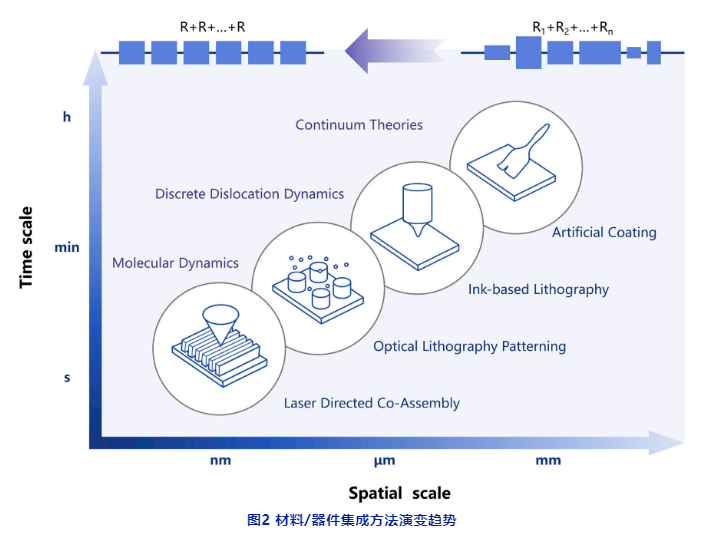
Figure 2 Evolution Trend of Material/Device Integration Methods
It is foreseeable that the laser-induced BCP assembly process is not only an important way to solve the reliability and consistency problems of miniature gas sensors, but also a common technology for the packaging manufacturing and industrial application of numerous photonic/electronic devices. At the same time, however, the application of external fields makes the entire research system more complex. Due to the continuous energy input and dissipation environment at the mesoscopic scale, the equilibrium conditions of the self-assembly system are destroyed, and the research object is no longer a classical equilibrium phase transition. Understanding those phase transition processes that rely on thermal density fluctuations becomes more challenging, such as: (i) obtaining the energy model of field-induced BCP directed assembly; (ii) near-field relaxation phenomena and dynamics of basic assembly units; (iii) artificial precise control methods for defect annihilation; (iv) new strategies for co-assembly of semiconductor sensitive material precursors and BCPs, etc.
Zhao Yuxin Associate Professor/Doctoral Supervisor, Xi'an Jiaotong University. His research focuses on "Materials and Devices for Industrial Safety Monitoring and Emergency Response," conducting full-chain R&D from basic research and key technology development to engineering demonstration. In recent years, his research interests have focused on intelligent sensing materials and devices and in-situ nano-measurement. To date, he has presided over the completion of more than 27 million yuan in various research projects from the National Natural Science Foundation of China, PetroChina, and Sinopec Group's Science and Technology Department. His achievements have won several awards, including the First Prize of the Sinopec Forward-looking Basic Research Science Award (2019) and the China Invention Patent Excellence Award (2022). He has been granted 18 Chinese invention patents and 2 patents in the US, Japan, Europe, and other countries (WIPO). In the past five years, he has published ACS Nano , Matter , Small Methods , Nano Research , Biosensor And Bioelectronics and other journals SCI more than 40 papers.
Zhao Yanli Lee Soo Ying Chair Professor, Nanyang Technological University, Singapore; Associate Head, School of Chemical & Biomedical Engineering; Assistant Dean, College of Science. He also serves as Chief Scientist at the Institute of Materials Research and Engineering (IMRE), Agency for Science, Technology and Research (A*STAR), Singapore. His main research interests include the design and preparation of novel self-assembled materials and their applications in biomedicine, catalysis, and green energy. He has published over 450 SCI papers with an h-index of 91. He has received numerous honors, including the Singapore National Research Foundation Fellowship (2010), MIT Technology Review's Innovators Under 35 (Singapore 2012), the Young Scientist Award of the Asian Photochemistry Association (2016), the ACS Applied Materials & Interfaces Young Investigator Award (2017), the Singapore National Research Foundation Investigatorship (2018), and the Clarivate Highly Cited Researcher (2018-2021). ACS Applied Materials & Interfaces Young Investigator Award (2017), Singapore National Research Foundation Investigatorship (2018), Clarivate Highly Cited Researcher (2018-2021), etc.


